VSD - Custom Layout (Udemy.com)
VLSI - This is where design meets fabrication
Created by: Kunal Ghosh
Produced in 2016
 What you will learn
- Draw layout from scratch, i.e. right from tech files to metal layer
- Understand each and every mask level, through appropriate fabrication steps
- Get to know how physical design flow communicates with CMOS fabrication process
- This is how 2 different industries communicate
 Quality Score
Overall Score : 90 / 100
 Live Chat with CourseDuck's Co-Founder for Help
 Course Description
While physical designers use all the outputs from experiments performed by fabrication department, this course will demonstrate the best of both worlds and connect them through exchange of certain files in certain format
This way, custom layout designers get to know an insight how does fabrication works, fabrication engineers get to know, how layout engineers uses their information. So this course is a place where both meet, talk and connect.
Also, the standard files needed to draw and simulate layout, are being taken, deduced and created from scratch and on the fly. This is, by far, the best way to understand layout, and I can promise you an exciting journey throughout this course
Course is structured to explain the CMOS packaging and fabrication steps in beginning, followed by software and files used to draw and simulate layout, and look into DRC rules.
Next, we will take a simple CMOS inverter and apply all concepts learned above. Finally, we will learn the 'Art of layout' using Euler's path. This is where you will solve complex functions and draw a layout out of it.
Welcome you all to my course and Happy Learning!!
See you in class!Who this course is for:
- Anyone curious to know the inception of layout
- Anyone curious to know the software behind layout drawing
- Anyone who wants to know how chip designers talk with chip fabrication department

*Some courses are excluded from this sale. Coupon not working? If the link above doesn't drop prices, clear the cookies in your browser and then click this link here.
Also, you may need to apply the coupon code directly on the cart page to get the discount.
 Instructor Details

- 4.5 Rating
 24 Reviews
Kunal Ghosh
Kunal Ghosh is the Director and co-founder of VLSI System Design (VSD) Corp. Pvt. Ltd. Prior to launching VSD in 2017, Kunal heldseveral technical leadership positions at Qualcomm's Test-chip business unit. He joined Qualcomm in 2010. He led the Physical design and STA flow development of 28nm, 16nm test-chips. At 2013, he joined Cadence as Lead Sales Application engineer for Tempus STA tool. Kunal holds a Masters degree in Electrical Engineering from Indian Institute of Technology (IIT), Bombay, India and specialized in VLSI Design & Nanotechnology.
Hands on with Technology @
1) MSM (mobile station mode chips) - MSM chips are used for CDMA modulation/demodulation. It consists of DSP's and microprocessors for running applications such as web-browsing, video conferencing, multimedia services, etc.
2) Memory test chips - Memory test chips are used to validate functionality of 28nm custom/compiler memory as well as characterize their timing, power and yield.
3) DDR-PHY test chips - DDR-PHY test chips are basically tested for high speed data transfer
4) Timing and physical design Flow development for 130nm MOSFET technology node till 16nm FinFET technology node.
5) "IR aware STA"
 Reviews

- Video Duration:
 4.5h
4.5h - Price: 11.99 Track Price 11.99 Track Price
- Provider:
 Udemy
Udemy - Year:
 2016
2016 - Language:
 English, English [Auto-generated]
 - Certificate:
 Yes
Yes

30-Day Money-Back Guarantee
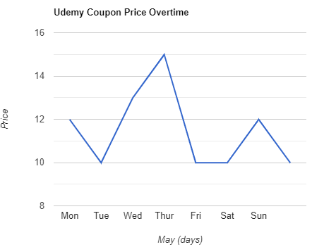
Udemy Coupon Price Tracker